PSU Efficiency and GaN
When Does GaN Make Sense for Improving Power Supply Efficiency?
Much has been made of wide bandgap (WBG) semiconductors, especially in the power supply industry. The listed advantages of Gallium Nitride (GaN) transistors include higher switching frequency, lower on-resistance, lower capacitance, and better thermal performance than traditional silicon MOSFETs. They can also be manufactured on silicon wafers like conventional semiconductor devices, allowing some parts of existing manufacturing chains to be used. In theory, this should help reduce the price of this new technology. However, GaN devices currently remain more expensive per device than traditional MOSFETs. So, when does it make sense to use GaN in a switching power supply design, and what improvements can be expected?
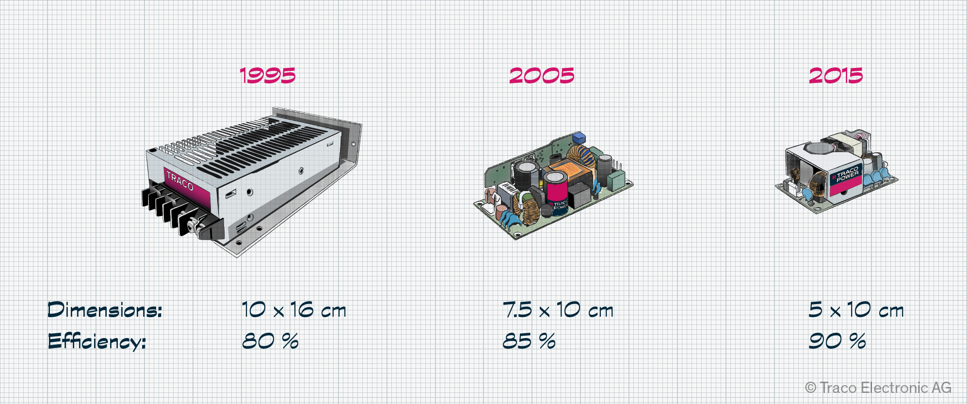
Over the past decades, the industry has made enormous progress in reducing power supply size and improving efficiency. Back in 1995, a 100 W solution had an area of 10 × 16 cm with an efficiency of 80%. Ten years later, the same power supply had a 7.5 × 10 cm footprint, and efficiency improved to 85%. By 2015, you’d be looking at 5 × 10 cm and 90% efficiency (Figure 1).
Faster switching speeds
During that time, we’ve moved from bipolar transistors, with a switching time of around 150 ns, to MOSFETs, with a 100 ns switching time, to high voltage superjunction “CoolMOS” that can switch in around 50 ns. And these improvements have made it possible to attain ever-higher switching frequencies. This enables the use of smaller capacitors, inductors, and transformers, enabling smaller products and designs with higher power densities and efficiencies.
GaN transistors can switch much faster than silicon MOSFETs, operating in the megahertz range rather than hundreds of kilohertz. So why aren’t we universally replacing silicon with GaN?
To answer this question, we need to understand each stage of a switching power supply (Figure 2). We have three functional blocks:
• Input filter and mains rectifier
• Active Power Factor Correction (PFC) to improve power factor and meet harmonics limits (EN 61000-3-2)
• Resonant converter (LLC)
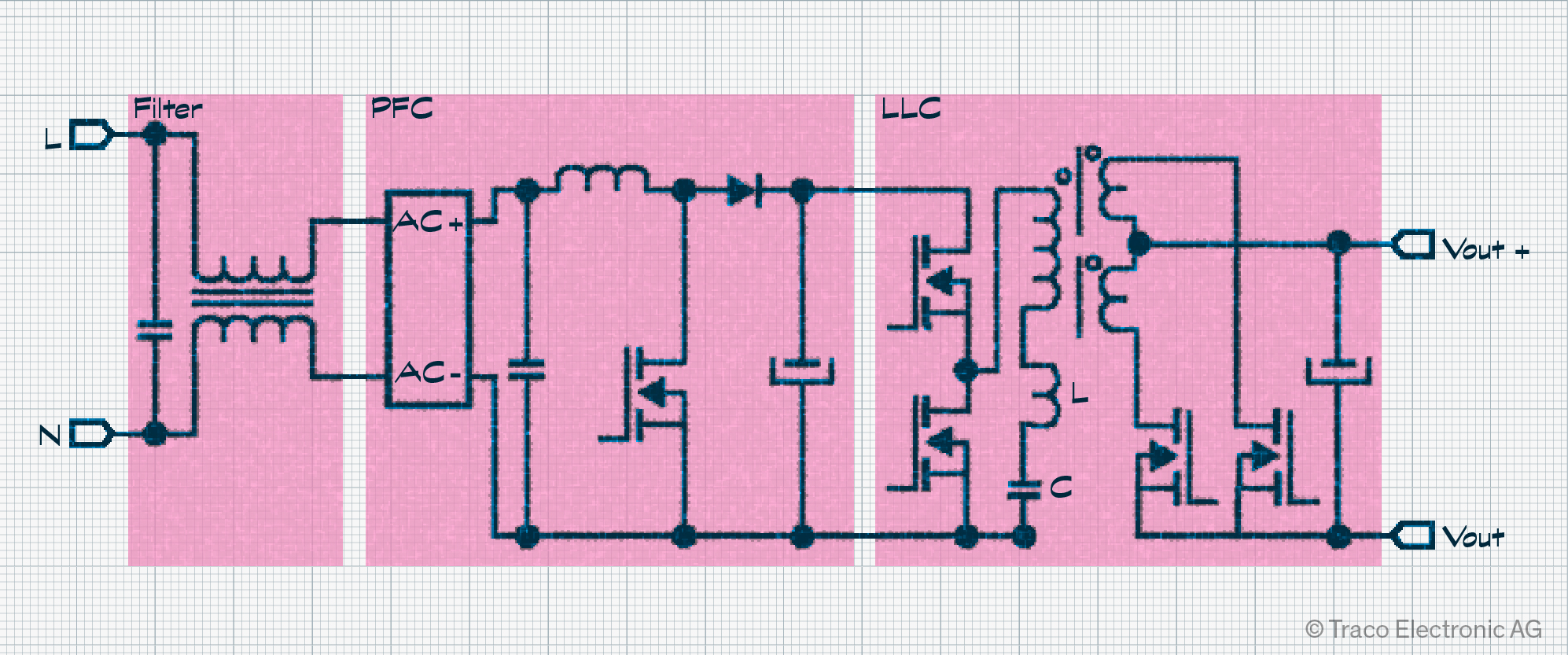
The PFC stage typically generates a relatively stable voltage of 380 V at its DC link capacitor. This is then converted to the desired isolated DC output voltage using four MOSFETs and a transformer.
The overall efficiency of a design like this could be as high as 93%. Of the 7% losses, 2% are attributed to the resonant converter and 5% to the PFC. 60% of these are due to switching losses.
Understanding switching losses
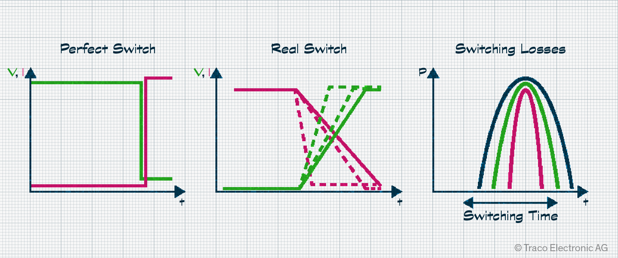
Switching losses occur because our MOSFETs and GaN transistors aren’t perfect switches. This means it takes time for them to move between their ON and OFF states. During this time, there is significant voltage and current across the device, with the resultant power dissipated as heat. So, the shorter this transition period, the lower the losses (Figure 3).
While today’s high-end MOSFETs have switching speeds of up to 50 ns, GaN devices can offer speeds of up to 7 ns. Since we have established that faster is better, the case for moving to GaN seems to have been made, should all the other device characteristics be broadly similar.
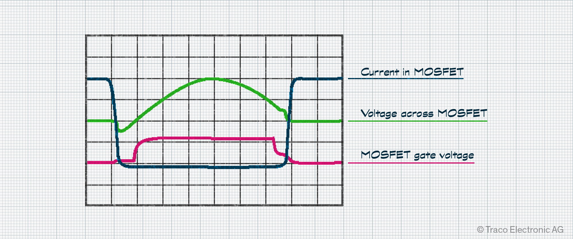
However, we need to examine our switching converter design in more detail. Let’s take the resonant converter first. At the moment of turn-on, the drain-source voltage of our MOSFET drops to zero (Figure 4). We also see that the current at this moment in time is almost zero. This is not a coincidence but a conscious choice in such designs to switch at the point of zero current. Because of this, resonant converters already have very low switching losses, meaning that a move to a faster-switching GaN device would have little impact.
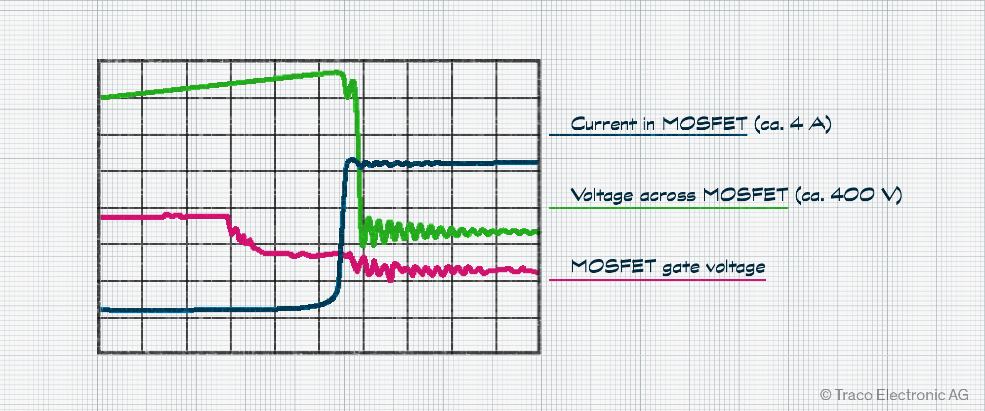
Perhaps there are improvements to be found in the PFC? At this point in this design, the voltage across the switch can be as high as 400 V, and the current through the switch can be as high as 4 A (Figure 5). With an overlap time of 30 ns at a switching frequency of 100 kHz, the switching power losses are around 4.8 W (4 A × 400 V × 30 ns × 100 kHz).
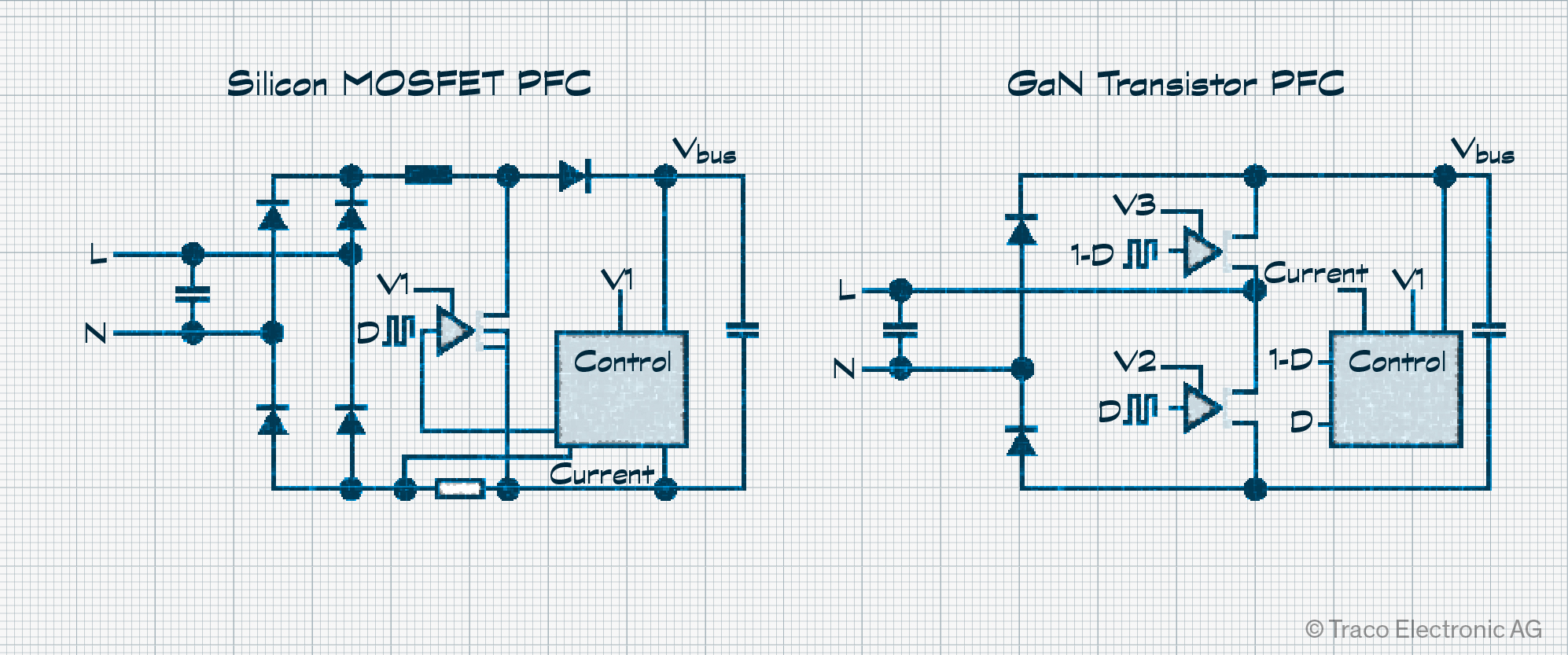
This means that GaN can make a difference here. A popular approach uses a totem pole topology (Figure 6). The bridge rectifier is removed and replaced by two diodes and two GaN transistors. A further benefit of this change is the lower, more controlled inrush current.
Implementing GaN in a 1000 W PFC design
In a 1000 W design operating at 800 W, experimentation shows that an 80 mΩ GaN transistor in such a totem pole PFC stage can achieve over 99% efficiency for an input voltage of 230 VAC. A classic PFC using silicon MOSFETs can only reach around 98%. However, at 110 VAC, almost no improvement over a silicon MOSFET is to be had, with both designs achieving around 96% efficiency. This is because the higher currents flowing lead to higher ohmic losses in the inductor (R × I2).
Such improvements also come at the expense of more complicated auxiliary circuitry. The two GaN transistors require three floating auxiliary supplies rather than a single non-floating supply for the silicon MOSFET design. The higher switching frequency also demands more design and testing effort to comply with radiated emissions limits.
When should I consider GaN?
Currently, GaN transistors don’t seem to offer any substantial benefit in the resonant converter stage of a switching power supply, as the existing switching losses are already low. Where it does make sense is in the PFC stage. With a top-end efficiency of 99% attainable, the efficiency for the entire power supply design can be pushed towards a respectable 96%.
However, this improvement comes at the cost of more engineering effort and complex filtering requirements. Viewed purely financially, the costs can be a factor of three to five times that of a silicon MOSFET design. Finally, second sourcing of GaN transistors remains challenging due to variations in each manufacturer’s recommended gate driver design, increasing the risks for PSU manufacturers.
Today, Traco Power engineers feel that GaN lends itself best to the PFC stage in PSU designs targeting at least 1000 W. To consider these new WBG devices in lower-power PSUs, the price of GaN transistors will need to drop further, something that typically happens as a technology matures.